How Scientists Find Atomic Defects in Computer Chips
A Cornell-led team has used electron ptychography to image 'mouse bite' defects inside next-generation chips for the first time — here is how the technique works and why it could transform semiconductor manufacturing.
The Invisible Enemy Inside Every Chip
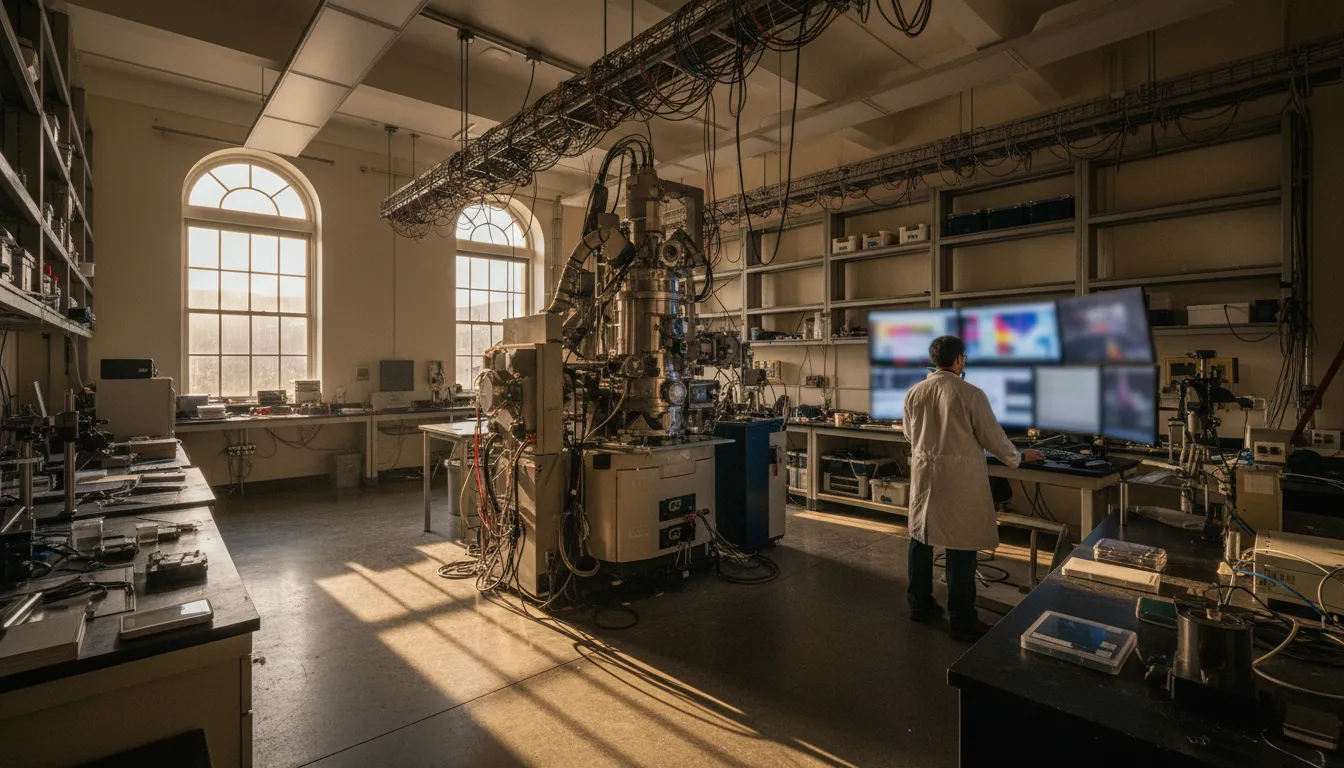
Every smartphone, laptop, and AI server runs on chips crammed with billions of transistors — each one smaller than a virus. At that scale, a single misplaced atom is not a curiosity; it is a defect that slows electrons, wastes energy, and can cause a chip to fail entirely. For decades, these atomic-scale flaws were essentially invisible. A 2026 breakthrough by a Cornell University-led team, in collaboration with chipmaker TSMC and materials firm ASM, changed that — using a computational imaging method called electron ptychography to reveal defects inside live transistors for the first time.
Why Defects Are So Hard to Spot
Modern chips are built at the 2-nanometer scale and below. The latest transistors, known as gate-all-around (GAA) devices, have silicon channels only 15 to 18 atoms wide. At that size, the surface of the channel — the path electrons must travel — is critically important. Any roughness, missing atom, or misplaced molecule scatters electrons, reducing speed and efficiency.
Researchers call these irregularities interface roughness. In a vivid nickname, the Cornell team dubbed the most visible form "mouse bite" defects — tiny notches eaten into the channel walls during manufacturing steps such as chemical etching, heat treatment, and layer deposition. In prototype chips, the team found that only about 60 percent of silicon atoms sat in a perfect, undisturbed structure; the rest were strained or roughened.
Traditional electron microscopes can image surfaces in two dimensions with high resolution, but peering inside a finished, buried transistor in three dimensions — without destroying it — was not previously possible.
What Is Electron Ptychography?
Ptychography is a computational imaging technique that fuses scanning microscopy with a branch of physics called coherent diffractive imaging. Here is how it works, step by step:
- A focused beam of electrons is fired at the sample (in this case, a real transistor inside a chip).
- As the beam moves across overlapping positions on the sample, a detector captures the full scattering pattern — the way electrons spread out after passing through the material.
- By comparing how those diffraction patterns shift between adjacent scan positions, a computer algorithm mathematically reconstructs both the shape of the electron beam and a three-dimensional map of the sample.
- The result is an image with sub-ångström lateral resolution — finer than the distance between two adjacent atoms — and enough depth information to locate defects buried inside the transistor.
The Cornell team used a specialized detector called an electron microscope pixel array detector (EMPAD) that captures the entire diffraction pattern at each position, rather than just a single intensity value. This flood of data — combined with iterative computational algorithms — is what makes the technique far more powerful than conventional microscopy.
Why Gate-All-Around Transistors Make This Urgent
The semiconductor industry shifted from FinFET to GAA architecture at the 3-nanometer node and beyond. In a FinFET, the gate (the switch that controls electron flow) wraps around three sides of a silicon fin. In a GAA device, the gate wraps around all four sides of a nanosheet channel, giving engineers tighter electrostatic control and allowing chips to run faster with less power leakage.
But that extra control comes with a price: the channels are extraordinarily thin, and their walls matter enormously. According to ASML, GAA transistors can deliver up to 15 percent higher speed or 30 percent better energy efficiency compared to 3nm FinFETs — but only if the channels are well-formed. Mouse bite defects eat directly into those gains.
Before electron ptychography, chipmakers relied on indirect statistical methods or destructive sample preparation (slicing chips open) to infer where defects formed during manufacturing. Neither approach can guide real-time process improvements in a modern fab.
What the Technique Reveals — and What Comes Next
Published in Nature Communications in early 2026, the Cornell study demonstrated that electron ptychography can map strain fields, interface roughness, and atomic displacements inside real GAA transistors without destroying them. That means engineers at TSMC and other fabs can now correlate specific manufacturing steps — which etch chemistry, which annealing temperature — with the defects that appear downstream.
The implications extend well beyond smartphones. AI data centers depend on densely packed chips running at peak efficiency; quantum computers require near-perfect silicon interfaces to maintain qubit coherence; automotive chips must meet strict reliability standards. Electron ptychography offers a universal quality-control tool for all of them.
The technique is still largely confined to research labs, and scanning a full chip at atomic resolution remains time-consuming. But as detectors grow faster and algorithms more efficient, the method is expected to move closer to the production line — giving chipmakers, for the first time, a true window into the atomic world hiding inside their products.