How High Bandwidth Memory Works—the Chip AI Can't Live Without
High Bandwidth Memory stacks DRAM dies vertically and connects them with thousands of through-silicon vias, delivering the massive data throughput that modern AI accelerators demand.
Why AI Needs a Different Kind of Memory
Every time a large language model generates a sentence or an image diffusion model renders a picture, billions of parameters must be shuttled between a processor and its memory. Conventional memory cannot keep up. The bottleneck is not computing power—it is memory bandwidth, the rate at which data travels to and from the chip. High Bandwidth Memory, or HBM, was engineered specifically to break that bottleneck, and it has become the single most sought-after component in the AI hardware stack.
Stacking Dies Like a Skyscraper
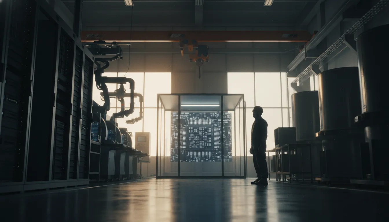
Traditional DRAM spreads memory chips side by side on a circuit board, connected by long traces that limit speed and waste energy. HBM takes a radically different approach: it stacks multiple DRAM dies vertically, like floors in a skyscraper, and bonds them together into a single compact package.
A modern HBM stack can contain eight or even twelve layers of DRAM. Each layer is connected to the ones above and below by thousands of through-silicon vias (TSVs)—microscopic copper-filled holes drilled straight through the silicon. These TSVs carry data vertically instead of horizontally, slashing the distance signals must travel and dramatically cutting power consumption.
The entire stack sits on a silicon interposer, a thin wafer that acts as a high-speed highway connecting the memory to the GPU or accelerator right next door. Because the data path is millimetres rather than centimetres long, HBM achieves bandwidth that would be physically impossible with conventional designs.
Numbers That Matter
Each HBM stack contains multiple independent channels operating in parallel. The current workhorse generation, HBM3E, delivers roughly 1.2 terabytes per second of bandwidth per stack with up to 36 GB of capacity. The next generation, HBM4, doubles the interface width from 1,024 bits to 2,048 bits and pushes bandwidth beyond 2 TB/s per stack—enough to feed the largest AI models during both training and inference.
For context, a single HBM4 stack moves data roughly 16 times faster than the fastest DDR5 module, while consuming significantly less energy per bit transferred. NVIDIA's Blackwell GPUs pair multiple HBM3E stacks for a combined bandwidth exceeding 8 TB/s per chip.
Why Manufacturing Is So Difficult
Building HBM is among the hardest tasks in semiconductor manufacturing. Each TSV must be etched, lined, and filled with copper at sub-micrometre precision across every layer. As stacks grow taller, alignment tolerances tighten and yield drops. A single defective via in a twelve-layer stack can render the entire unit useless.
Only three companies in the world mass-produce HBM: SK Hynix, Samsung, and Micron. SK Hynix currently dominates with roughly 57 percent of global HBM shipments, followed by Samsung at around 35 percent and Micron at approximately 11 percent, according to Counterpoint Research. All three have sold out their entire production capacity through the end of the year.
The Memory Wall and AI's Future
Engineers call the growing gap between processor speed and memory speed the "memory wall." As AI models scale from billions to trillions of parameters, the wall gets higher. HBM is the industry's primary tool for scaling it.
Bank of America estimates the HBM market will reach $54.6 billion in 2026, a 58 percent jump from the prior year, with projections pointing toward $100 billion by 2028. The technology's trajectory mirrors AI's own explosive growth: every new generation of accelerator demands more stacks, more layers, and more bandwidth.
HBM will not remain the only solution forever—researchers are exploring alternatives such as compute-in-memory and optical interconnects—but for the foreseeable future, these tiny towers of stacked silicon remain the chokepoint that determines how fast artificial intelligence can think.